Activity
Mon
Wed
Fri
Sun
Mar
Apr
May
Jun
Jul
Aug
Sep
Oct
Nov
Dec
Jan
Feb
What is this?
Less
More
Memberships
Fresuelectronics.com
1.6k members • Free
2 contributions to Fresuelectronics.com

Jul '24 •
KiCad Project Template - Lesson 3
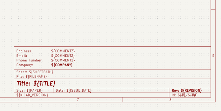
Hi, I'm at Lesson 3 - Creating Project Templates. To make a good template for my project I read the documentation related to Drawing Sheet Editor: https://docs.kicad.org/8.0/en/pl_editor/pl_editor.html. I quickly found that unfortunately it's outdated. I created a issue on KiCad website: https://gitlab.com/kicad/services/kicad-doc-website/-/issues/38. I see that there is no big activity there, maybe here we can discuss about creating a good template? Some of my personal preferences: - Change every size to mils as schematic grid is in mils - Margins 250 mils left, 285 mils right, 800 mils top and 892.99 mils bottom to adjust for page size - Page size A3 - unfortunately it's in metric so margins are adjusted - Text width and height 50 mils (Title 80x80 mils), step between rows 100 mils - Block size 2000 x 2000 mils - Text margin from the left 50 mils - Grid step 50 mils * Edit nr 1 - adjusted margins
1 like • Jul '24
Update: KiCad team answered my issue and updated the documentation! Check it out: https://docs.kicad.org/8.0/en/pl_editor/pl_editor.html

Feb '24 •
Maximizing the Value of Schematic Design in Professional Projects
One of the misconceptions I had about designing a schematic when I started in this field was that the schematic is only a representation of the electrical connections between components. However, as I began to gain more experience, I quickly noticed that this approach was only suitable for my home projects, not for the professional world, where different people are involved, and good documentation becomes crucial. The schematic is, in fact, the part of the project that coordinates the layout. This means that the schematic should guide us during the layout. The schematic is not only a representation of the electrical circuit but also our guide on how and where components should be located, and connected. For designers who work in a small company where they have to wear many hats and take care of the schematics, layout, testing, and software, this might seem like a waste of time. I understand this, as I also started this way. However, in larger companies, you usually have people who specialize in different parts of the project. For example, one person designs the schematics, and another person designs the layout. The idea is that you want to build the schematics in a way that allows another person to build the layout without needing your input. Also, if you don't do this, and you leave the company, then your designs become unusable for the company, which then has to go back and reverse engineer your work. The better you are at designing your schematics, the more valuable the work you do becomes, and the more valuable you become to the company. This also means the more value they can compensate you with.
1 like • Jul '24
For schematics, I was always annoyed at the description table in the bottom right corner. When reviewing a project, it seems unreadable: the margins and text width are off, and the information is outdated. When I see that this table is properly taken care of, I can quickly get basic information about a project and then get into details.
1-2 of 2

@ukasz-wojnarowski-6490
Electronics Design Engineer with 7.5 years of experience. Working in Home Appliances and Automotive Industries.
Active 5d ago
Joined Jun 25, 2024
Poland