
Write something

Oct '25 •
Facing an EMC test is one of the most stressful moments for any electronic engineer.
Facing an EMC test is one of the most stressful moments for any electronic engineer. It’s that nerve-wracking time when your design, which has worked flawlessly until now, is put under the toughest scrutiny. You’re waiting for the report, pass or fail, or, if you’re at the lab, you watch the results live while your heart pounds like a drum roll. This is the moment when ego, pride, and months of work are on the line. Because it’s not just about you. The whole team is behind you, but you’re the face of the design. Failure is simply not an option. The budget won’t allow another failed EMC test. Neither will the project stakeholders, who are already pushing to launch the product. And yet, here’s the truth: most engineers were never properly taught how to design with EMC in mind. At school, we learned equations that seemed disconnected from real-world PCB design. We fell back to outdated classical circuit theory, building like plumbers with pipes instead of engineers working with electromagnetic fields. We were told that understanding EM fields requires a PhD in math. That EMC is “too complex”, almost like black magic. But it doesn’t have to be this way. That’s why we created the EMC/EMI Design Course. This course was built by engineers, for engineers. No fluff, no theory that never translates to practice. Instead, you’ll get: - A clear, practical method to design boards that pass EMC faster. - Tools, techniques, and strategies you can apply immediately in your projects. - A proven system that eliminates costly trial-and-error fixes and unpractical last-minute patches. This is real engineering knowledge you’ll use every day, from design to lab testing to final compliance. If you’re ready to stop fearing EMC tests and start controlling EMI with confidence, click below and join the course today. 👉 fresuelectronics.com/emi-design-course Don’t let another project be at risk. Master EMI control once and for all.
0
0

Jul '25 •
📢 Become the Go-To Specialist in EMI Control & PCB Design.
This is the #1 community for electronic engineers to help you: - Master EMI Control in Electronic Design - Close the gap between theory and practice - Earn more by becoming a skilled EMI specialist - Learn Electromagnetic Compatibility without a PhD - Grow into senior roles - Get career & business support - Start your freelancing/consulting business What you get : - Direct expert support - Personal advice from Dario Fresu - Monthly 1:1 coaching calls - Immediate access to all courses & workshops - Personal design reviews - Private Q&A forum - Templates, tools, and checklists - 100s hours of curated training - Career/freelancing package - Structured learning path & certificates - Real project walkthroughs & case studies - Private Specialist Community 🚨 Limited seats available at €99/month or €999/year (save 2 months ). Cancel anytime. Join us here: EMC/EMI Control Academy
2
0
Jul '24 •
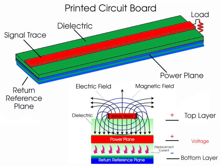
Be aware of using Power Planes as Return Reference Planes!
Back when I started designing PCBs I heard it was pretty common to use power planes as Return Reference Planes (RRP), and I still see that this is widely used in the industry. An example is the "classic" 4-layer stackup: - SIGNAL - POWER - "GROUND" - SIGNAL One of the problems we have with this stackup is that the signal on the top layer uses the power plane as a path for the current to close the loop and return to the source. But how does it actually close the loop if the POWER plane is DC disconnected from the "GROUND" plane? Unfortunately, it does so through the displacement current, which has to cross the impedance between the POWER plane and the "GROUND" plane. This means that when this happens, the current flowing through the impedance between the planes will generate a voltage drop, which will impact the whole board and eventually affect EMI. And yes, I know the common recommendation is to add decoupling capacitors, but unfortunately, this will only work up to certain frequencies due to the impedance profile of the capacitor. The best scenario is to have the Return Reference Plane adjacent to the signal layer. However, if we are forced to use the power plane option, make sure that the impedance between the POWER plane and the "GROUND" plane is as small as possible so that the voltage drop is minimized. One way to achieve this is to reduce the distance between the planes as much as possible, which will increase the interplane capacitance and lower its impedance. I hope this helps, Dario
Oct '24 •
Don't wait 10 years...
You don't have to be 10 years into PCB Design to become an EMI specialist. In fact, I bet you already have a lot of knowledge on the topic, but what I see people struggling with the most is putting things together. I know because I was in the same place too. My approach was to first design the schematics, and then convert it into PCB Layout. Pretty straightforward, right? More or less... Until the board would suddenly freeze, or some LED would randomly switch on and off, or some components would start to heat up randomly. I mean, it was that bad. Little did I know that the problem was actually in how my layout was designed. Not because the connections from point to point weren’t correct or robust, but because the project wasn’t designed with electromagnetic fields in mind. The good part is that I didn’t have to go through complex equations to make a U-turn and set the project right from the start. In fact, I dare to say that the concepts are pretty simple to grasp. And if you want to know what these concepts are, I’m sharing them here for free: CLASSROOMS Enjoy, Dario ---- P.S. If you want to take your career to the next level and become an EMI specialist yourself, comment with the word "SPECIALIST," and I'll guide you on what to do next.

Feb '24 •
FREE Electromagnetic Compatibility (EMC) eBook 👇
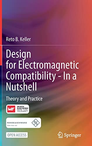
I know many PCB Designers and Product Designers experience issues with electromagnetic compatibility, particularly understanding why some products fail and the fundamental principles behind it. This book will explain the 'why' and the 'how,' and it's completely free to download. Here is the link to download the book: https://link.springer.com/book/10.1007/978-3-031-14186-7 Hope you enjoy it. Dario By the way, if your goal is to become a PCB expert, if you want to design boards right the first time, and if you want to understand why some designs fail in the first place, then you need to check this out: 👉 PCB Hackers Premium Community
1-20 of 20
powered by
skool.com/pcb-hackers-8346
Master professional electronic design and Printed Circuit Boards (PCB). Learn about EMC/EMI, signal & power integrity, high-speed design.
Suggested communities
Powered by