Activity
Mon
Wed
Fri
Sun
Jan
Feb
Mar
Apr
May
Jun
Jul
Aug
Sep
Oct
Nov
Dec
What is this?
Less
More
Memberships
Fresuelectronics.com
1.6k members • Free
2 contributions to Fresuelectronics.com

Aug 21 •
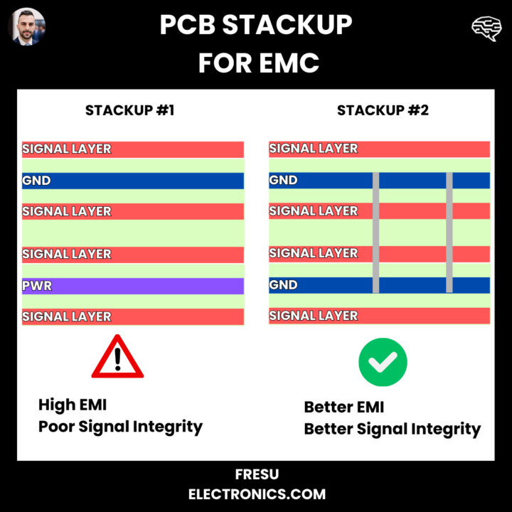
EMC/EMI Bites: 6-Layer Stackup – Exactly How Not to Use Them
Scrolling the web this morning, here’s what I saw: 1. SGN 2. GND (Plane) 3. SGN 4. SGN 5. PWR (Plane) 6. SGN My heartbeat dropped for a second. Another PCB designer is about to waste thousands of dollars on EMC tests, simply because he followed these recommendations from a random internet post, without applying critical thinking from first principles. The idea that this is a good 6-layer stackup comes from the misconception that power planes are valid reference planes. They are not. Why? Because it’s not only about reference, it’s also about the return path. Return current needs to complete its loop. It cannot terminate on a PWR layer; it has to return to the GND plane. So, besides the 1st and 3rd layers, all other layers in this stackup will see extra conductors in their return path to GND: - Layer 4 will see Layer 3, - Layer 5 will see Layers 4 and 3, - Layer 6 will see Layers 5, 4, and 3. This means there will be interference between these layers and their signals. Remember: the energy and the fields live in the space between the conductors, not inside the conductors themselves! The conductors only guide the fields. When designing a stackup, choose layers in pairs so that every signal or power layer has a return and reference plane (RRP) adjacent to it. In this case, that means GND. So how should we fix this stackup to reduce interference and improve Signal Integrity and EMI? Swap the PWR layer with a GND layer, and stitch the two GND planes together with vias. This makes both planes equipotential, while also providing proper return and reference paths when signals transition between layers. Think of it as channeling the fields between conductors, not inside a single conductor. If these concepts aren’t clear yet and you want to dive deeper, check out my EMC/EMI design course. It explains in detail why this happens and how to design stackups that actually work. Visit fresuelectronics.com To electromagnetic enlightenment,

0 likes • Aug 21
i saw it too. I was in the same heart-stopping mode.

Jun '24 •
Connection between the Ethernet transmitter and the Ethernet switch on the same board?
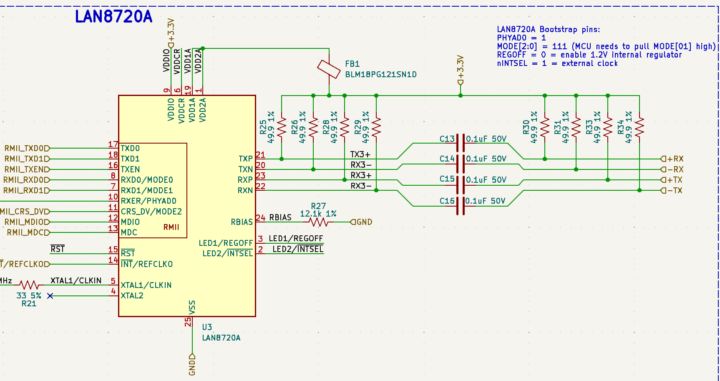
Hello everyone, I am working on a project that involves an Ethernet Switch (RTL8305NB-VB-CG) and an Ethernet Transceiver (LAN8720A). They will be connected on a single PCB. Does anyone know if it is mandatory to use isolation transformers (for TX, RX), or is it not required since they are on the same PCB? I would be grateful if someone could provide a correct connection schematic. I am not 100% sure, but some application notes suggest that isolation capacitors for each line are sufficient if they are on the same PCB. I am connecting them this way(attached screenshot), but I want to be completely sure. I will be happy to any help!😊 My references: Capacitive Coupling Ethernet Transceivers without Using Transformers (microchip.com) AN-1519 DP83848 PHYTER® Transformerless Ethernet Operation (Rev. A) Tuning the 8255x Controller’s Equalizer Application Note 435 (intel.com) https://www.ti.com/lit/an/slla310/slla310.pdf?ts=1719011312654 https://www.analog.com/media/en/technical-documentation/application-notes/ee-269.pdf https://ww1.microchip.com/downloads/en/Appnotes/VPPD-01534.pdf [second screenshot] Thank you.
2 likes • Jun '24
They are required by standard, if you plan to use only with your device you can give a try, but i still do not recommend it.
2 likes • Jun '24
@Nazar Melnichek Don't forget to route them as differential pairs with 100 Ohms trace impedance.
1-2 of 2

Active 17d ago
Joined Jun 25, 2024